APB4 GPIO
Fully Parameterized APB4 General-Purpose-IO
License Terms:
Non-Commercial License
This project is maintained by:
RoaLogic
APB4 General Purpose Input/Output (GPIO) Datasheet
Contents
Introduction
The APB4 GPIO Core is fully parameterised core designed to provide a user-defined number of general purpose, bidirectional IO to a design.
The IO are accessible via an AMBA APB v2.0 Specification interface – typically referred to as APB4 – with the core operating synchronously at the rising edge of the APB4 Bus Clock.
GPIO inputs to the core may operate asynchronously to the core and will be automatically synchronised to the bus clock. Outputs may be configured to operate in push-pull mode or open-drain.
GPIO inputs may also be individually configured to generate a level or edge sensitive interrupt. A single IRQ output is provided to connect to the host.
Features
-
Compliant with AMBA APB v2.0 Specification
-
User-defined number of Bi-directional General Purpose IO
-
Automatic synchronisation of General Inputs to Bus Clock
-
Each General Output configurable as push-pull or open-drain
-
Programmable IRQ generation
-
Each General Input individually configurable as a level or edge triggered interrupt.
Specifications
Functional Description
The Roa Logic APB4 GPIO is a configurable, fully parameterized soft IP to enable general connectivity to a APB4 based Master (Host) It is fully compliant with the AMBA APB v2.0 bus protocols.
The IP contains a single Master Interface to connect to the APB4 Host and a user defined number of General Purpose IO, configurable as a bi-directional bus as shown below:
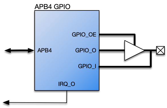
The core operates synchronously with the APB4 Bus Clock. The core synchronises all GPIO_I inputs to the APB4 Bus Clock domain.
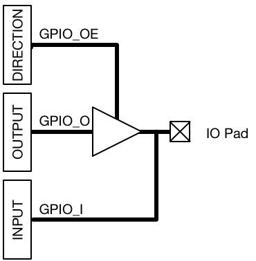
Operating Modes
The core supports bidirectional IO pads as shown in Figure 3, where each IO can be programmed to operate in push-pull or open-drain mode. The mode of each IO is defined via the MODE register.
| Note: | |
|---|---|
| IO Pads are not implemented within the APB4 GPIO core – this technology specific capability is the responsibility of the designer. |
Push-Pull Mode
In push-pull mode, each bit of the GPIO_O bus is driven from an internal OUTPUT register and GPIO_OE is controlled via the DIRECTION register
Logically the push-pull mode is configured as follows:
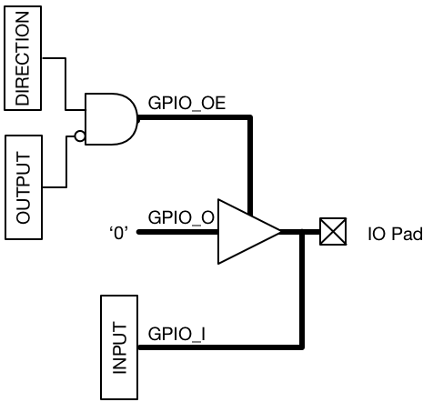
Open-Drain Mode
In open-drain mode, each bit of GPIO_O is always driven low (‘0’) and individual GPIO_OE signals enable (i.e. Logic ‘0’) or Hi-Z (Logic ‘1’) the output buffer corresponding to the value of the OUTPUT register.
Pad Inference
The inclusion of technology specific IO Pads is not part of the APB4 GPIO core and instead left to the designer. Pads may be behaviourally inferred however as follows:
PAD[n] = GPIO_OE[n] ? GPIO_O[n] : 1’bz;
GPIO_I[n] = PAD[n];
Configurations
Introduction
The Roa Logic AHB-Lite APB4 GPIO is a fully configurable General Purpose Input/Output core. The core parameters and configuration options are described in this section.
Core Parameters
| Parameter | Type | Default | Description |
|---|---|---|---|
PDATA_SIZE |
Integer | 8 | APB4 Data Bus & GPIO Size |
INPUT_STAGES |
Integer | 2 | Number of GPIO_I input synchronisation stages |
PDATA_SIZE
The PDATA_SIZE parameter specifies the width of the APB4 data bus and corresponding GPIO interface width. This parameter must equal an integer multiple of bytes.
INPUT_STAGES
The APB4 GPIO inputs are sampled on the rising edge of the APB4 bus clock (PCLK). As these inputs may be asynchronous to the bus clock, the core automatically synchronises these signals and the INPUT_STAGES parameter determines the number of synchronisation stages. Increasing this parameter reduces the possibility of metastability due to input signals changing state while being sampled, but at the cost of increased latency. The default value of the INPUT_STAGES parameter is 2
Control Registers
The APB4 GPIO core implements user accessible registers as described below:
| Register | Address | Access | Function |
|---|---|---|---|
MODE |
Base + 0x0 |
Read/Write | Push-Pull or Open-Drain Mode |
DIRECTION |
Base + 0x1 |
Read/Write | Output Enable control |
OUTPUT |
Base + 0x2 |
Read/Write | Output Data Store |
INPUT |
Base + 0x3 |
Read Only | Input Data Store |
TRIGGER_TYPE |
Base + 0x4 |
Read/Write | Trigger Type |
TRIGGER_LVL0 |
Base + 0x5 |
Read/Write | Trigger Sense 0 |
TRIGGER_LVL1 |
Base + 0x6 |
Read/Write | Trigger Sense 1 |
TRIGGER_STATUS |
Base + 0x7 |
Read/Write | Trigger Status |
IRQ_ENABLE |
Base + 0x8 |
Read/Write | Enable Interrupts |
MODE
MODE is a PDATA_SIZE bits wide Read/Write register accessible at the address 0x0. Each bit of the register individually sets the operating mode for each signal of the GPIO_O and GPIO_OE buses as either push-pull or open drain, as follows:
| MODE[n] | Operating Mode |
|---|---|
| 0 | Push-Pull |
| 1 | Open Drain |
In push-pull mode, data written to the OUTPUT register directly drives the output bus GPIO_O. The DIRECTION register is then used to enable GPIO_O to drive the IO pad when set to ‘Output’ mode (‘1’).
In open-drain mode, GPIO_O is connected such that the IO Pad is driven low (’0’) when the output is ’0’ and is Hi-Z, pulled high via an external resistor, when the output is ’1’.
DIRECTION
DIRECTION is a PDATA_SIZE bits wide active-high read/write register, accessible at the address 0x1, and controls the output enable bus GPIO_OE[n], effectively controlling if PAD[n] operates as an input or an output.
| DIRECTION[n] | Direction |
|---|---|
| 0 | Input |
| 1 | Output |
OUTPUT
OUTPUT is a PDATA_SIZE bits wide read/write register accessible at the address 0x2.
Each bit of the OUTPUT register specifies the PAD[n] level when GPIO[n] is programmed as an output. Writing a ‘0’ drives a low level onto PAD[n], whereas writing a ‘1’ drives a ‘1’ (push-pull) or Hi-Z(open-drain) onto PAD[n].
INPUT
INPUT is a PDATA_SIZE bits wide read-only register accessible at the address 0x3.
On the rising edge of the APB4 Bus Clock (PCLK) input data on pins GPIO_I is sampled, synchronised and stored in the INPUT register where it may be read via the APB4 Bus Interface.
TRIGGER_TYPE
TRIGGER_TYPE is a PDATA_SIZE bits wide Read/Write register accessible at address 0x4.
Each bit of the register sets if a GPIO_I input bit is configured as a level or edge sensitive interupt trigger as defined below:
| TRIGGER_TYPE[n] | Type |
|---|---|
| 0 | Level |
| 1 | Edge |
TRIGGER_LVL0 and TRIGGER_LVL1
TRIGGER_LVL0 and TRIGGER_LVL1 are PDATA_SIZE bits wide Read/Write registers accessible at addresses 0x5 and 0x6 respectively.
Each bit of the TRIGGER_LVL0 and TRIGGER_LVL1 registers set the trigger sense of an interrupt input on GPIO_I. Based on the corresponding TRIGGER_TYPE bit defining a GPIO_I[n] input as level or edge triggered, an interrupt is triggered when the GPIO_I[n] input is low and/or high, or on a rising and/or falling edge transition as documented in the tables below.
Setting both registers to all ’0’ means that triggers are disabled and no interrupt will be generated from any GPIO_I input. This is the default state.
| TRIGGER_LVL0[n] | Level Triggered | Edge Triggered |
|---|---|---|
| 0 | no trigger when low | no trigger on falling edge |
| 1 | trigger when low | trigger on falling edge |
| TRIGGER_LVL1[n] | Level Triggered | Edge Triggered |
|---|---|---|
| 0 | no trigger when high | no trigger on rising edge |
| 1 | trigger when high | trigger on rising edge |
TRIGGER_STATUS
TRIGGER_STATUS is a PDATA_SIZE bits wide Read/Write register accessible at address 0x7.
Each bit of TRIGGER_STATUS register is set (’1’) if an trigger condition is detected on the corresponding GPIO_I[n] input according to the settings of TRIGGER_TYPE and TRIGGER_LVL0/1. If both TRIGGER_STATUS[n] and IRQ_ENABLE[n] are set (’1’), an interrupt is generated on the IRQ_O pin.
TRIGGER_STATUS may be read to determine if a trigger condition has occured on the corresponding input. Writing a ’1’ to TRIGGER_STATUS[n] will clear the status, unless a new trigger is detect simultaneously, in which case TRIGGER_STATUS[n] will remain set.
| TRIGGER_STATUS[n] | Status |
|---|---|
| 0 | no trigger detected/irq pending |
| 1 | trigger detected/irq pending |
IRQ_ENABLE
IRQ_ENABLE is a PDATA_SIZE bits wide Read/Write register accessible at address 0x8.
Each bit of IRQ_ENABLE determines if the IRQ_O pin will be asserted when a trigger condition occurs on the corresponding GPIO_I[n] input, and so enabling if interupts are generated from the APB4 GPIO core.
| IRQ_ENABLE[n] | Definition |
|---|---|
| 0 | disable irq generation |
| 1 | enable irq generation |
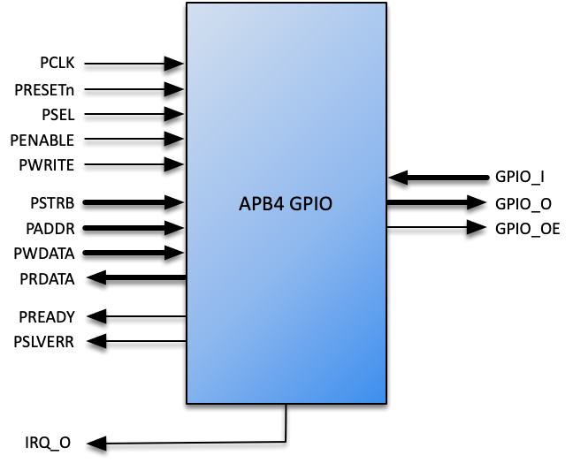
Interfaces
APB4 (Peripheral) Interface
The APB4Interface is a regular APB4 Master Interface. All signals defined in the protocol are supported as described below. See the AMBA APB Protocol v2.0 Specifications for a complete description of the signals.
| Port | Size | Direction | Description |
|---|---|---|---|
PRESETn |
1 | Input | Asynchronous active low reset |
PCLK |
1 | Input | Clock Input |
PSEL |
1 | Output | Peripheral Select |
PENABLE |
1 | Output | Peripheral Enable Control |
PWRITE |
1 | Output | Write Select |
PSTRB |
PDATA_SIZE/8 |
Output | Byte Lane Indicator |
PADDR |
PADDR_SIZE |
Output | Address Bus |
PWDATA |
PDATA_SIZE |
Output | Write Data Bus |
PRDATA |
PDATA_SIZE |
Input | Read Data Bus |
PREADY |
1 | Input | Transfer Ready Input |
PSLVERR |
1 | Input | Transfer Error Indicator |
PRESETn
When the active low asynchronous PRESETn input is asserted (‘0’), the APB4 interface is put into its initial reset state.
PCLK
PCLK is the APB4 interface system clock. All internal logic for the APB4 interface operates at the rising edge of this system clock and APB4 bus timings are related to the rising edge of PCLK.
PSEL
The APB4 Bridge generates PSEL, signaling to an attached peripheral that it is selected and a data transfer is pending.
PENABLE
The APB4 Bridge asserts PENABLE during the second and subsequent cycles of an APB4 data transfer.
PWRITE
PWRITE indicates a data write access when asserted high (‘1’) and a read data access when de-asserted (‘0’)
PSTRB
There is one PSTRB signal per byte lane of the APB4 write data bus (PWDATA). These signals indicate which byte lane to update during a write transfer such that PSTRB[n] corresponds to PWDATA[(8n+7):8n].
PADDR
PADDR is the APB4 address bus. The bus width is defined by the PADDR_SIZE parameter and is driven by the APB4 Bridge core.
PWDATA
PWDATA is the APB4 write data bus and is driven by the APB4 Bridge core during write cycles, indicated when PWRITE is asserted (‘1’). The bus width must be byte-aligned and is defined by the PDATA_SIZE parameter.
PRDATA
PRDATA is the APB4 read data bus. An attached peripheral drives this bus during read cycles, indicated when PWRITE is de-asserted (‘0’). The bus width must be byte-aligned and is defined by the PDATA_SIZE parameter.
PREADY
PREADY is driven by the attached peripheral. It is used to extend an APB4 transfer.
PSLVERR
PSLVERR indicates a failed data transfer when asserted (‘1’). As APB4 peripherals are not required to support this signal it must be tied LOW (‘0’) when unused.
GPIO Interface
| Port | Size | Direction | Description |
|---|---|---|---|
GPIO_I |
PDATA_SIZE |
Input | Input Signals |
GPIO_O |
PDATA_SIZE |
Output | Output Signals |
GPIO_OE |
PDATA_SIZE |
Output | Output Enable Signal |
IRQ_O |
1 | Output | IRQ Output Signal |
GPIO_I
GPIO_I is the input bus. The bus is PDATA_SIZE bits wide and each bit is sampled on the rising edge of the APB4 bus clock PCLK. As the inputs may be asynchronous to the bus clock, synchronisation is implemented within the core.
GPIO_O
GPIO_O is the output bus and is PDATA_SIZE bits wide. Data is driven onto the output bus on the rising edge of the APB4 bus clock PCLK.
GPIO_OE
GPIO_OE is an active-high Output Enable bus and is PDATA_SIZE bits wide.
The specific functionality of the GPIO_OE bus is defined by the MODE register. In push-pull mode it is used to enable a bidirectional output buffer whose input is driven the GPIO_O bus
In open-drain mode the GPIO_OE bus is used to enable a logic ‘0’ to be driven from the GPIO_O bus, and a logic ’1’ by disabling (‘Hi-Z’) the output buffer.
IRQ_O
IRQ_O is a single bit output which is asserted (’1’) when a valid interrupt is triggered on GPIO_I. The conditions for the assertion of IRQ_O are programmable via a control register interface.
Resources
Below are some example implementations for various platforms. All implementations are push button, with no effort undertaken to reduce area or improve performance.
| Platform | DFF | Cells | Memory | Perf. (MHz) | Comments |
|---|---|---|---|---|---|
| Cyclone V | 140 | 96ALUTs | 0 | 0 | PDATA_SIZE=8 |
Note: This table will be updated as more examples are compiled.
Revision History
| Date | Rev. | Comments |
|---|---|---|
| 13-Oct-2017 | 1.0 | Initial Release |
| 25-May-2020 | 2.0 | Added interrupt capabilities |