RISC-V Timer
RISC-V Compliant Timer IP
License Terms:
Non-Commercial License
This project is maintained by:
RoaLogic
AHB-Lite Timer Datasheet
Contents
Product Brief
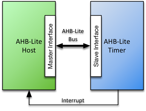
The Roa Logic AHB-Lite Timer IP is a fully parameterized soft IP implementing a user-defined number of timers and functions as specified by the RISC-V Privileged 1.9.1 specification.
The IP features an AHB-Lite Slave interface, with all signals defined in the AMBA 3 AHB-Lite v1.0 specifications fully supported, supporting a single AHB-Lite based host connection. Bus address & data widths as well as the number of timers supported are specified via parameters.
The timebase of the timers is derived from the AHB-Lite bus clock, scaled down by a programmable value.
The module features a single Interrupt output which is asserted whenever an enabled timer is triggered
Features
-
AHB-Lite Interface with programmable address and data width
-
User defined number of counters (Up to 32)
-
Programmable time base derived from AHB-Lite bus clock
Specification
Functional Description
The AHB-Lite Timer IP is a fully parameterised Timer-tick core, featuring a single AHB-Lite Slave interface and a single multiplexed Interrupt output signal.
The Timer IP is intended to generate CPU interrupts at regular time intervals, for timed events such as time keeping, task/context switches, and sleep().
The number of timers and Address & Data width of the AHB-Lite interface are specified via parameters defined at compile time.
The time base of the timers is common to all timers and defined at runtime by writing to the PRESCALER register. Individual timer alarms may then set via the TIMECMP[n] registers. All timers are permanently enabled however a separate IENABLE register allows any triggered counter output to be masked.
The user may determine both the status of the TIMERS including which timer has generated an interrupt via a read operation to the AHB-Lite interface.
Configuration
Introduction
The size and implementation style of the timer module is defined via HDL parameters as specified below.
Core Parameters
| Parameter | Type | Default | Description |
|---|---|---|---|
TIMERS |
Integer | 3 | Number of Timers |
HADDR_SIZE |
Integer | 32 | Width of AHB-Lite Address Bus |
HDATA_SIZE |
Integer | 32 | Width of AHB-Lite Data Buses |
TIMERS
The parameter TIMERS defines the number of timers supported and thereby the number of TIMECMP registers implemented by the core. Values between 1 and 32 are supported, with the default defined as ‘3’.
HADDR_SIZE
The HADDR_SIZE parameter specifies the address bus size to connect to the AHB-Lite based host.
HDATA_SIZE
The HDATA_SIZE parameter specifies the data bus size to connect to the AHB-Lite based host. The maximum size supported is 64 bits.
Core Registers
| Register | Address | Size | Access | Function |
|---|---|---|---|---|
PRESCALER |
Base + 0x00 | 32bits | Read/Write | Timebase |
IPENDING |
Base + 0x08 | 32bits | Read Only | Interrupt Pending |
IENABLE |
Base + 0x0C | 32bits | Read/Write | Interrupt Enable |
TIME |
Base + 0x10 | 64bits | Read/Write | Timer Register |
TIMECMP[n] |
Base + 0x18+8n | 64bits | Read/Write | Compare Value |
Note: ‘n’ represents an integer for 0 to TIMERS-1.
PRESCALER
The Timer module operates synchronously with the AHB-Lite bus clock input HCLK. A 32 bit PRESCALER register enables the time base for the timers to be less than that of HCLK by dividing this clock frequency by the value of PRESCALER + 1.
For example: If PRESCALER=3, the timer will increment every PRESCALER+1=4 cycles of HCLK, setting the time base to HCLK/4 Hz.
The default value of PRESCALER=0, thereby setting the timer clock frequency equal to the bus (HCLK) frequency. The TIME counter starts incrementing once the register PRESCALER is written to for the first time.
Note: The value of PRESCALER value can only be defined once after the peripheral is released from reset.
IPENDING
IPENDING is a 32-bit read-only register that indicates if a timer interrupt is pending.
Each bit of the IPENDING register corresponds to one timer with the position of each bit indicating the associated timer. E.g. bit zero indicates the interrupt status of Timer[0]. IPENDING bits associated with unimplemented timers are tied low (‘0’)
An interrupt pending bit is set when the value of TIMECMP[n] equals the value of TIME. It is cleared by a write to the associated TIMECMP[n] register, as specified in the RISC-V privileged spec 1.9.1.
IENABLE
IENABLE is a 32-bit Read/Write register, where each bit of the register is a dedicated ’Interrupt Enable’ bit for each time. The bit position indicates the associated timer. E.g. Interrupt Enable for Timer[0] is located at bit position 0.
Only TIMERS bits are implemented with the remaining MSBs always read as ’0’. A write to the unused MSBs has no effect.
An interrupt is generated when a bit of IPENDING is set and its associated IENABLE bit is also set. This allows the core to be used in (1) pure POLL mode, where the CPU polls the status of the bits to determine if a timer event happened, (2) pure interrupt driven mode, where each timer can generate an interrupt, or (3) a combination of the above.
TIME
The TIME register is a common 64-bit high-resolution time-keeping counter used by all timers. It is the basis for the RDCYCLE instruction as specified in the RISC-V privileged spec 1.9.1 and may be written to also in accordance with the RISC-V specification.
The time base for the TIME register is derived from the AHB-Lite bus clock HCLK and is defined as:
FreqTIME = FreqHCLK / (PRESCALER+1)
The counter starts incrementing once the register PRESCALER is written to for the first time.
TIMECMP[n]
For each timer (as defined by the parameter TIMER) there is a dedicated 64 bit Time Compare register which defines when the IPENDING bits are asserted
These registers are denoted as TIMECMP[n], where ‘n’ is an index from 0 to TIMERS-1, and are located consecutively in the address space according to the formula:
Base Address of TIMECMP[n] = 0x18 + 8n
For example, TIMECMP[0] is located at address 0x18, TIMECMP[1] at 0x20, TIMECMP[5] at 0x28 etc.
The IPENDING bit associated with the TIMECMP register is set when the TIMECMP[n] value equals the value of TIME.
IPENDING[n] = (TIMECMP[n] == TIME)
Writing the TIMECMP[n] register clears bit ‘n’ of the IPENDING register.
Interfaces
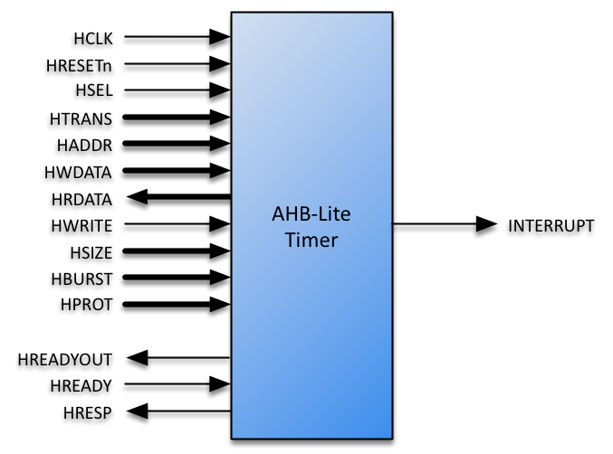
AHB-Lite Interface
The AHB-Lite interface is a regular AHB-Lite slave port. All signals are supported. See the AMBA 3 AHB-Lite Specification for a complete description of the signals.
| Port | Size | Direction | Description |
|---|---|---|---|
HRESETn |
1 | Input | Asynchronous active low reset |
HCLK |
1 | Input | Clock Input |
HSEL |
1 | Input | Bus Select |
HTRANS |
2 | Input | Transfer Type |
HADDR |
HADDR_SIZE |
Input | Address Bus |
HWDATA |
HDATA_SIZE |
Input | Write Data Bus |
HRDATA |
HDATA_SIZE |
Output | Read Data Bus |
HWRITE |
1 | Input | Write Select |
HSIZE |
3 | Input | Transfer Size |
HBURST |
3 | Input | Transfer Burst Size |
HPROT |
4 | Input | Transfer Protection Level |
HREADYOUT |
1 | Output | Transfer Ready Output |
HREADY |
1 | Input | Transfer Ready Input |
HRESP |
1 | Output | Transfer Response |
HRESETn
When the active low asynchronous HRESETn input is asserted (‘0’), the interface is put into its initial reset state.
HCLK
HCLK is the interface system clock. All internal logic for the AHB-Lite interface operates at the rising edge of this system clock and AHB bus timings are related to the rising edge of HCLK.
HSEL
The AHB-Lite interface only responds to other signals on its bus – with the exception of the global asynchronous reset signal HRESETn – when HSEL is asserted (‘1’). When HSEL is negated (‘0’) the interface considers the bus IDLE.
HTRANS
HTRANS indicates the type of the current transfer as shown in the table below:
HTRANS |
Type | Description |
|---|---|---|
00 |
IDLE |
No transfer required |
01 |
BUSY |
Connected master is not ready to accept data, but intents to continue the current burst. |
10 |
NONSEQ |
First transfer of a burst or a single transfer |
11 |
SEQ |
Remaining transfers of a burst |
HADDR
HADDR is the address bus. Its size is determined by the HADDR_SIZE parameter and is driven to the connected peripheral.
HWDATA
HWDATA is the write data bus. Its size is determined by the HDATA_SIZE parameter and is driven to the connected peripheral.
HRDATA
HRDATA is the read data bus. Its size is determined by the HDATA_SIZE parameter and is sourced by the connected peripheral.
HWRITE
HWRITE is the read/write signal. HWRITE asserted (‘1’) indicates a write transfer.
HSIZE
HSIZE indicates the size of the current transfer as shown in table [tab:HSIZE]:
HSIZE |
Size | Description |
|---|---|---|
000 |
8 bit | Byte |
001 |
16 bit | Half Word |
010 |
32 bit | Word |
011 |
64 bits | Double Word |
100 |
128 bit | |
101 |
256 bit | |
110 |
512 bit | |
111 |
1024 bit |
HBURST
HBURST indicates the transaction burst type – a single transfer or part of a burst.
HBURST |
Type | Description |
|---|---|---|
000 |
SINGLE |
Single access |
001 |
INCR |
Continuous incremental burst |
010 |
WRAP4 |
4-beat wrapping burst |
011 |
INCR4 |
4-beat incrementing burst |
100 |
WRAP8 |
8-beat wrapping burst |
101 |
INCR8 |
8-beat incrementing burst |
110 |
WRAP16 |
16-beat wrapping burst |
111 |
INCR16 |
16-beat incrementing burst |
HPROT
The HPROT signals provide additional information about the bus transfer and are intended to implement a level of protection.
| Bit# | Value | Description |
|---|---|---|
| 3 | 1 | Cacheable region addressed |
| 0 | Non-cacheable region addressed | |
| 2 | 1 | Bufferable |
| 0 | Non-bufferable | |
| 1 | 1 | Privileged Access |
| 0 | User Access | |
| 0 | 1 | Data Access |
| 0 | Opcode fetch |
HREADYOUT
HREADYOUT indicates that the current transfer has finished. Note, for the AHB-Lite PLIC this signal is constantly asserted as the core is always ready for data access.
HREADY
HREADY indicates whether or not the addressed peripheral is ready to transfer data. When HREADY is negated (‘0’) the peripheral is not ready, forcing wait states. When HREADY is asserted (‘1’) the peripheral is ready and the transfer completed.
HRESP
HRESP is the instruction transfer response and indicates OKAY (‘0’) or ERROR (‘1’).
Timer Interface
TIMER_INTERRUPT
TIMER_INTERRUPT is a single output signal that is asserted the following conditions are both met:
-
Any bit of the
IPENDINGregister is asserted -
The corresponding bit of the
IENABLEregister is also asserted.
This may also be written as:
TIMER_INTERRUPT <= IPENDING & IENABLE
Resources
Below are some example implementations for various platforms. All implementations are push button, no effort has been undertaken to reduce area or improve performance.
| Platform | DFF | Logic Cells | Memory | Performance (MHz) |
|---|---|---|---|---|
(This table will be updated in future revisions of the datasheet)
Revision History
| Date | Rev. | Comments |
|---|---|---|
| 24-Oct-2017 | 1.0 | Initial Release |